
In the shadowy world of Cold War aerospace and nuclear deterrence, the greatest threat to electronic systems was not software bugs or enemy interception—it was the environment itself. High-energy radiation, capable of scrambling bits and inducing catastrophic latch-up events in standard silicon, posed a terminal risk to America’s most sensitive strategic assets. To solve this, Sandia National Laboratories in Albuquerque, New Mexico, embarked on an ambitious mission: building a custom, radiation-hardened semiconductor fabrication facility from the ground up. The crown jewel of this endeavor was the SA3000, a reimagined version of the venerable Intel 8085 processor that would go on to govern the firing mechanisms of nuclear warheads and the navigation of deep-space probes.
The Genesis of the "Rad-Hard" Mandate
By the late 1970s, the gap between commercial off-the-shelf (COTS) electronics and the needs of national security had become an unbridgeable chasm. Standard integrated circuits (ICs) were designed for consumer reliability, not for survival in the vicinity of a nuclear detonation or the harsh vacuum of deep space. Sandia, tasked with the stewardship of the nation’s nuclear stockpile, recognized that if they wanted technology that could withstand extreme ionizing radiation, they would have to manufacture it themselves.
While companies like Fairchild and Allied Signal handled high-volume packaging, the actual silicon wafer fabrication was brought in-house. In 1978, the laboratory inaugurated its fab facility using a 10-micron process on 2-inch wafers. While this was several generations behind the "state-of-the-art" commercial nodes of the time, the objective was never density or speed—it was survivability. By 1982, the facility had evolved to a 4-inch wafer system utilizing a 2-micron process, setting the stage for one of the most critical contributions to space exploration: the Galileo mission.
For the Galileo Jupiter probe, Sandia was tasked with re-engineering standard processors—including the RCA 1802—into radiation-hardened variants. The scope of the project was massive; over 50,000 ICs were manufactured, tested, and vetted to ensure the probe could survive the intense radiation belts of the Jovian system.
Chronology: From Concept to Strategic Deployment
The development of the SA3000 did not happen in a vacuum; it was part of a broader trajectory of Cold War engineering.
- 1978: Sandia establishes its internal fabrication facility, focusing on 10-micron, radiation-hardened processes.
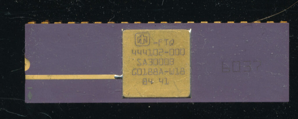
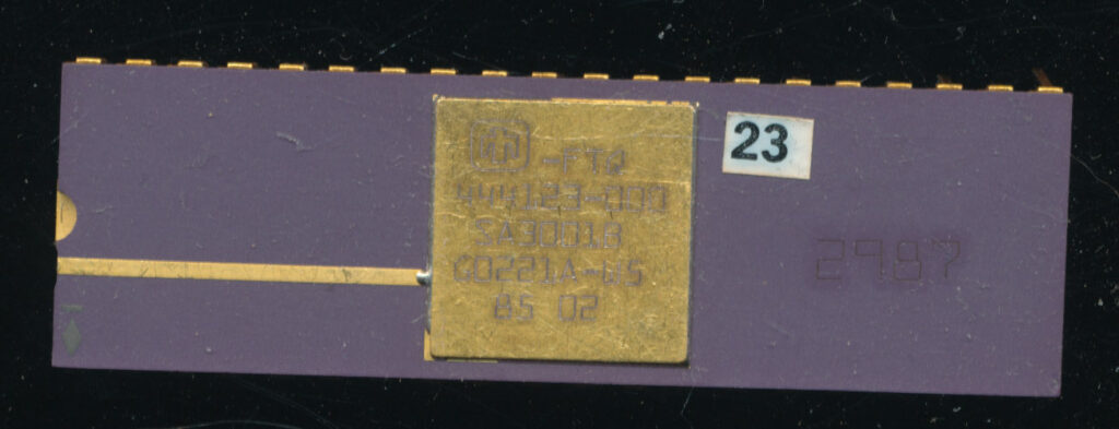
- 1982: Upgraded to a 4-inch wafer process (2-micron). Sandia begins the conversion of the Intel 8085 architecture into the CMOS-based SA3000.
- 1984: The SA3000 reaches maturity. The processor, built with 18,000 transistors (a significant jump from the 6,500 in the original NMOS 8085), enters production.
- 1985: Administrative friction emerges as the U.S. government mandates that Allied Signal take over the management of the fabrication facility, a move that would later be cited by insiders as a catalyst for production slowdowns.
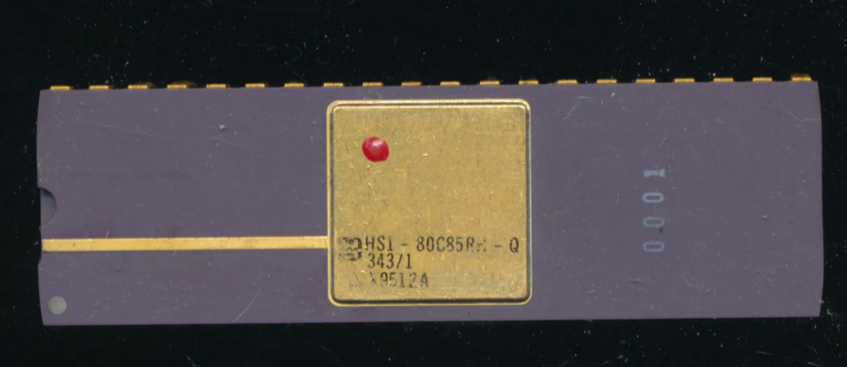
- 1990: The SA3000 is officially commercialized via a partnership with Harris (later Intersil/Renesas), emerging as the HS1-80C85RH.
- 1990: The Combined Release and Radiation Effects Satellite (CRRES) launches, utilizing the SA3000 to monitor radiation effects in orbit.
The Architecture of Survival: Designing the SA3000
The transition from Intel’s NMOS 8085 to the Sandia SA3000 was a masterclass in semiconductor hardening. The original 8085 relied on HMOS technology, which is inherently susceptible to the types of latch-up events caused by ionizing radiation. Sandia’s solution was a total shift to a hardened CMOS (Complementary Metal-Oxide-Semiconductor) process.
Hardening Techniques
Designing for radiation hardness is an exercise in paranoia. The engineers at Sandia employed several specific strategies:
- N-on-N+ Epitaxial Substrates: This structure provides a low-resistance path to ground, effectively suppressing the parasitic thyristor effects that cause latch-up.
- Guard Rings: Extensive guard-banding was utilized around every transistor to isolate components from the substrate.
- Hardened Oxides: By precisely controlling production temperatures and oxidation rates, engineers minimized the "trapped charge" effect that occurs when radiation strikes insulating layers.
- Substrate Biasing: The design ensured that power and ground were contacted to the substrate and well structures as frequently as possible, minimizing the distance an electrical surge could travel before being dissipated.
The resulting SA3000 operated between 4.5V and 11V. This wide voltage range was not merely for flexibility; it provided "headroom." As a chip is exposed to radiation, the propagation delay of its transistors increases—effectively slowing it down. By operating at higher voltages, the circuit maintained enough timing margin to continue functioning long after a standard 5V chip would have missed a clock cycle.

Supporting Infrastructure and Ecosystem
The SA3000 was not a standalone hero; it required an entire ecosystem of support chips to function in a mission-critical environment. Sandia produced the SA3001 (a hardened version of the Intel 8155 RAM/IO/Timer), the SA3002 (the 8355 ROM/IO chip), and the SA3026 (the 8212 latch).
These chips were essentially the backbone of the "War Reserve" stockpile. Sandia maintained a strategic inventory of these components to ensure that, regardless of commercial market volatility or geopolitical shifts, the U.S. military could service its existing nuclear delivery systems, such as the W88 warhead utilized on the Trident II submarine-launched ballistic missiles. The SA3000 became the "brains" of these reentry vehicles, handling the critical altitude and fuzing calculations that determine whether a device functions as intended.
The Impact of Outsourcing: The Allied Signal Transition
In the mid-1980s, a pivotal administrative shift occurred. The Department of Energy and the federal government pushed to transition the fab management to a private contractor, settling on Allied Signal. For the scientists and engineers at Sandia, this was a period of significant frustration. Allied Signal, while a titan of industry, lacked the specialized, niche experience required to run a high-security, rad-hard fab.
The transition led to immediate bottlenecks. The highly tuned, bespoke processes developed by Sandia’s in-house team were difficult to translate to a corporate management style focused on commercial efficiency. While the facility continued to produce, the agility and rapid prototyping capabilities that Sandia had spent nearly a decade refining were significantly hampered for several years.
Implications: The Legacy of "Obsolete" Tech
When Harris commercialized the SA3000 as the HS1-80C85RH in 1990, it signaled a shift in how radiation-hardened technology was viewed. The Harris parts were lower-spec than the original Sandia-made chips—limited to 5V and a maximum speed of 2MHz—yet they found a massive market in the aerospace industry.
The long-term implication of the SA3000 is the validation of "proven" technology. While modern processors have millions of times the processing power of an 8085, they are also exponentially more fragile. A single cosmic ray striking a modern 3nm transistor can cause a bit-flip. The SA3000, by contrast, is a tank. It was designed to function in a world where the laws of physics are actively trying to destroy it.
Reliability vs. Performance
The design goal for the SA3000 was 100,000 rads of total ionizing dose (TID). In practice, the chip far exceeded this, withstanding 1,000,000 rads with only a 25% performance degradation, and 3,000,000 rads with a 40% drop. To put this in perspective, a dose of 1,000 rads is generally fatal to a human being. The SA3000’s ability to remain operational at 3,000 times the lethal human dose illustrates why this architecture remained relevant for decades.
Conclusion: The Enduring Silicon
The story of the Sandia SA3000 is a testament to the fact that in national security, the "newest" technology is not always the best technology. The project demonstrated that by combining rigorous design, specialized fabrication processes, and an uncompromising focus on environmental resilience, it is possible to create electronics that are effectively immune to the hazards of their environment.
While the 8085 architecture is long since "obsolete" by modern desktop computing standards, it remains a foundational piece of the U.S. nuclear deterrent and the history of space exploration. The SA3000 remains a benchmark for what can be achieved when the goal is not to maximize profit or performance, but to guarantee that when the signal is sent, the machine will respond—no matter what the environment throws at it.
